-
6000+Plant area
-
2000+Area of purification room
-
10+Doctor's and master's
degree employees -
50+Company Honors and
Qualifications


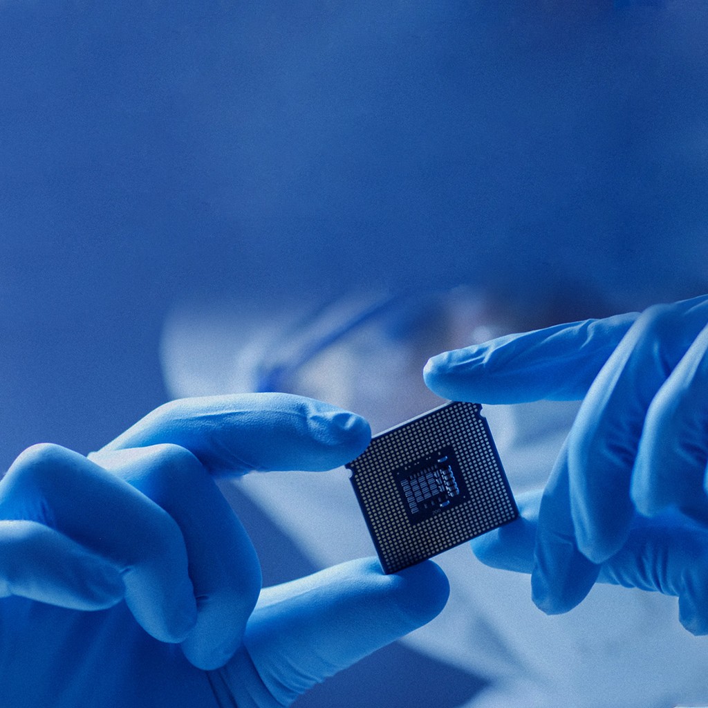

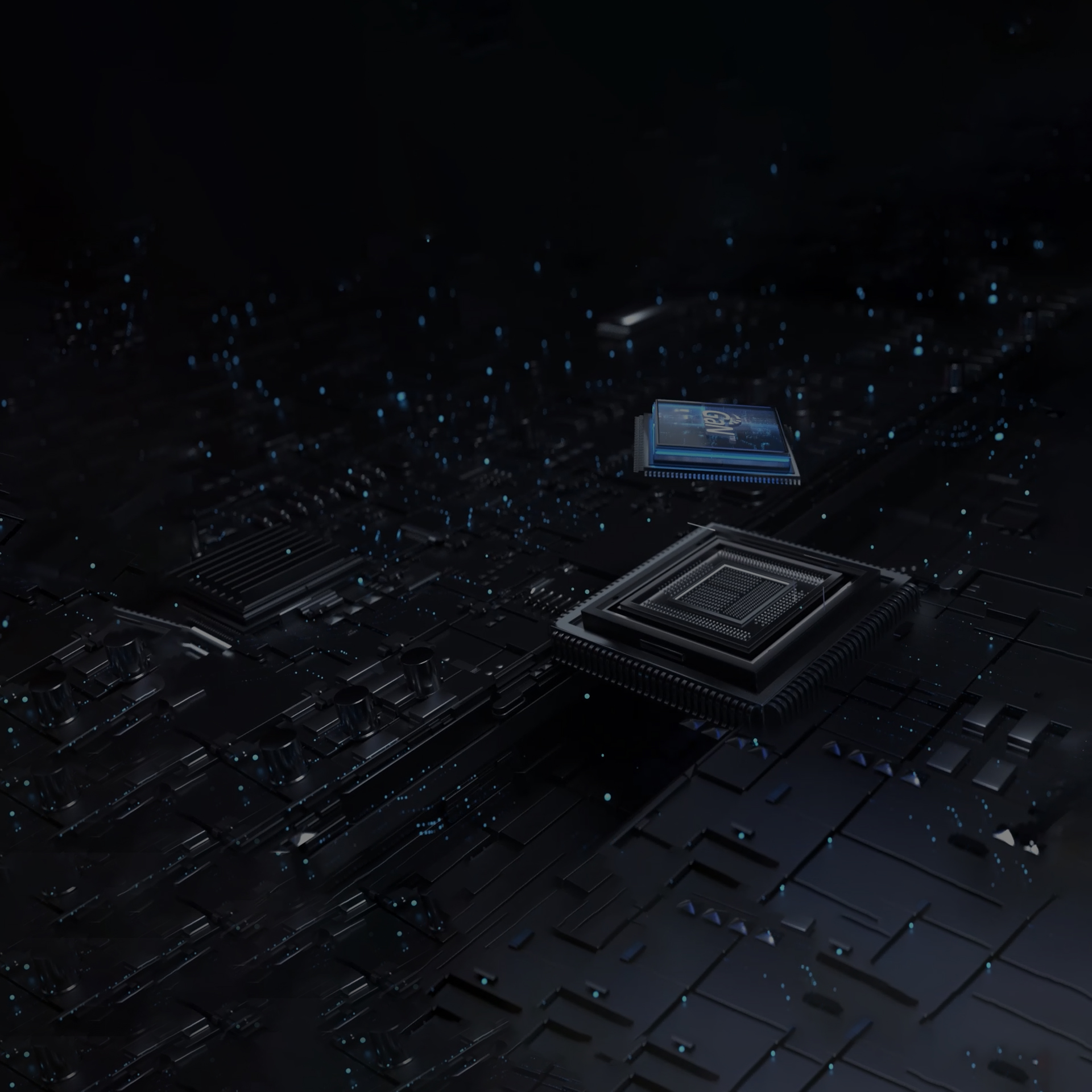
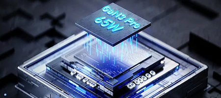
Small and medium power GaN Schottky diode series: small and medium power general Schottky switching diodes (breakdown voltage 20-300V) and small power RF Schottky diodes (operating frequency 10MHz-28GHz); GaN RF power amplifier: 5G communication with (2.4-3.5GHz, 24.5-29.8 GH) RF power amplifier; GaN power switching devices GaN power switching devices: current 3-30A, voltage 200-650V.
 More
More
GaN UV light-emitting diode series: UV LED chips including UVA (365nm), UVB (310nm) and UVC (275nm) products, according to market demand, the wavelength and luminous power can be adjusted; GaN laser diode series: 80-100mW blue (440-460nm) and green (510-520nm) lasers.
More
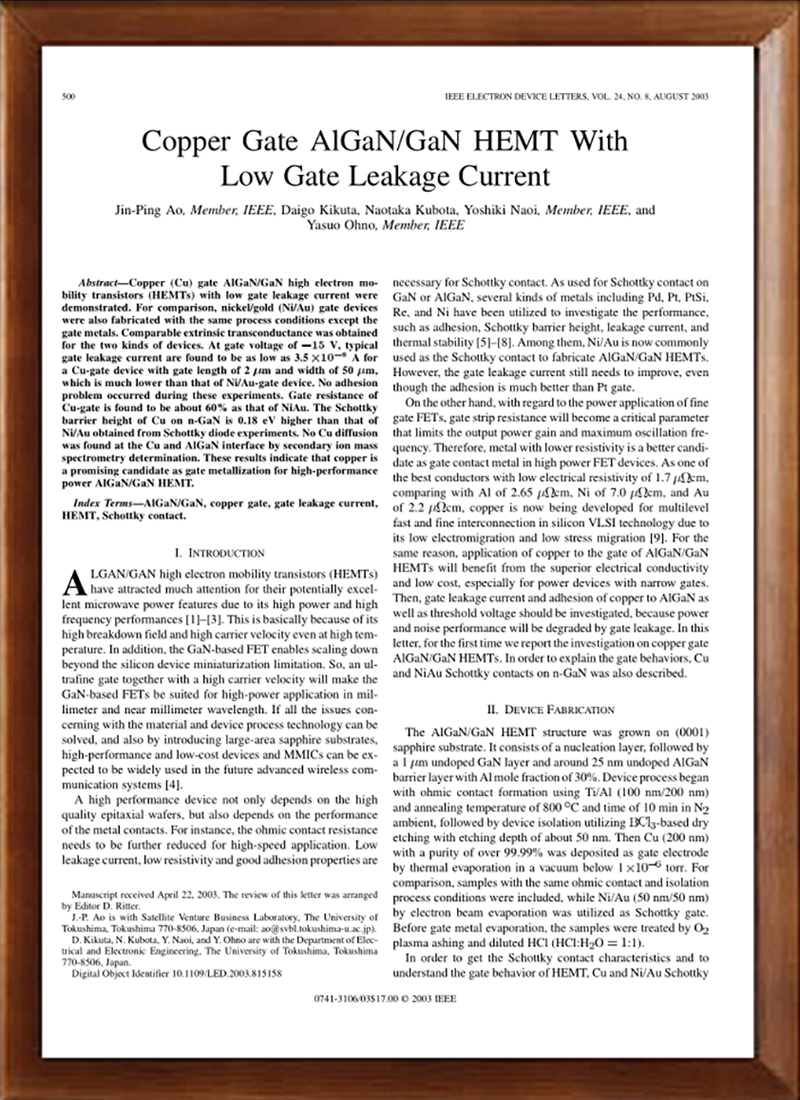
The company gathers technical experts from mainland China, Japan and Taiwan who have been working in the field of gallium nitride for decades, as well as young talents such as doctors and masters. With three levels of talent echelon, has rich technical accumulation and continuous innovation ability. With Japan, Taiwan, South Korea and other overseas colleges and universities, related enterprises have a stable cooperative relationship.

Honors and Qualifications
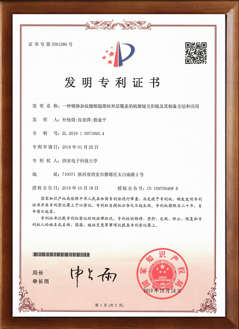
Honors and Qualifications
Honors and Qualifications

Honors and Qualifications
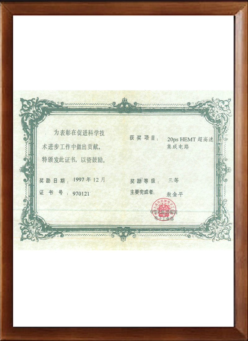
Honors and Qualifications

Honors and Qualifications

Ningbo City Science and Technology Innovation 2025 major special project
The core of a semiconductor diode is a PN junction, which is characterized by the characteristics of a PN junction - unidirectional conductivity. The voltammetric characteristic curve is often used to
 More
More
Different semiconductor device preparation has different morphological requirements for semiconductor materials, including single crystal wafers, milled wafers, polished wafers, thin films, etc. Diffe
 More
More
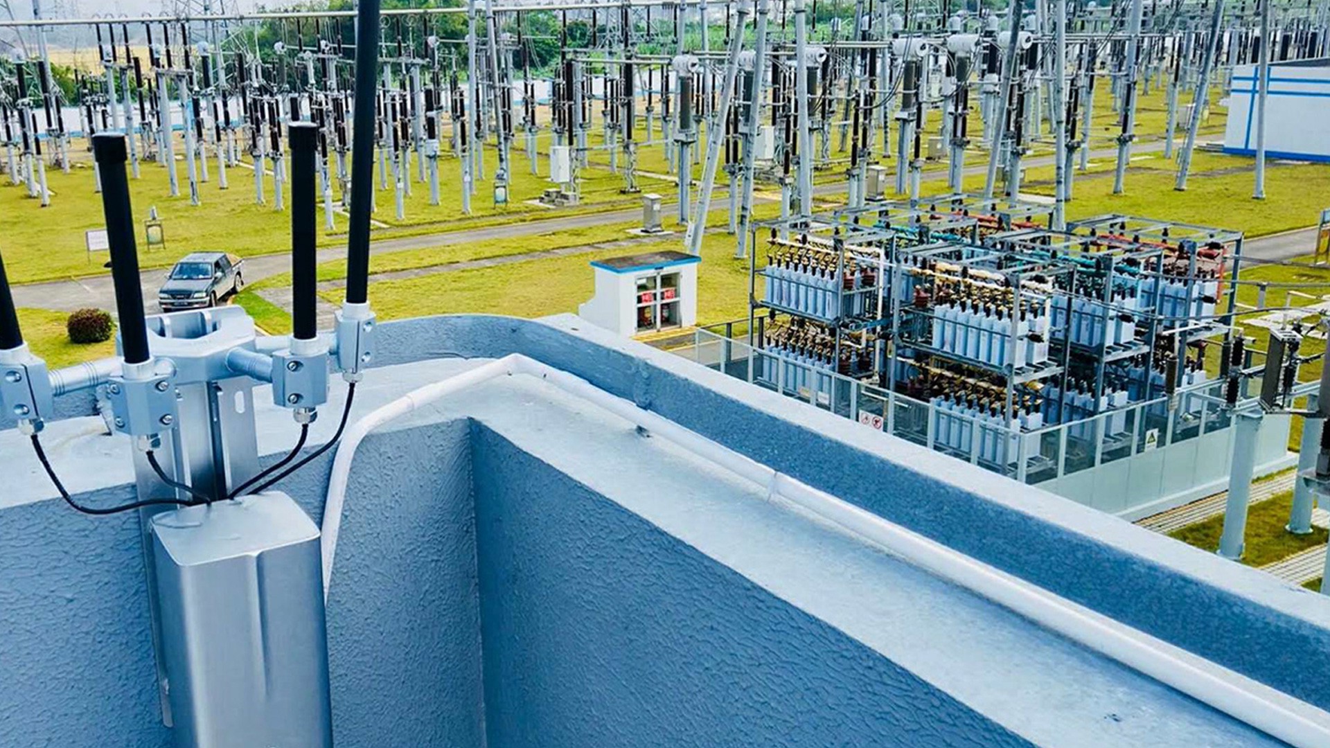
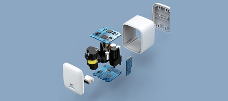
5G commercialization will drive the development of 5G cell phones, base stations, VR/AR devices, and emerging applications such as Industry 4.0, autonomous driving and healthcare.
More


Take a sweep